
The anticipation for the Nintendo Switch 2 – or whatever it ends up being called – is reaching levels of mania I didn’t quite anticipate, but a major leak last week of what appear to be prototype components gives us our first hard evidence of what form the machine may actually take, while hinting at the components within.
So, what have we got? Essentially, there are a number of factors to consider. First of all, there has been the relentless and quite remarkable pursuit of Switch 2 facts and rumours from the members of the Famiboard forums, who have chased down every leak and compiled a compelling and almost complete specification. Thanks to tracking shipping manifests out of Taiwan, they have discovered a lot about the technical make-up of Nintendo’s next generation hardware right down to the component level. It’s because of this information that it can be determined that the leak last week is genuine – or at least as accurate as an old prototype dating from October 2023 can be.
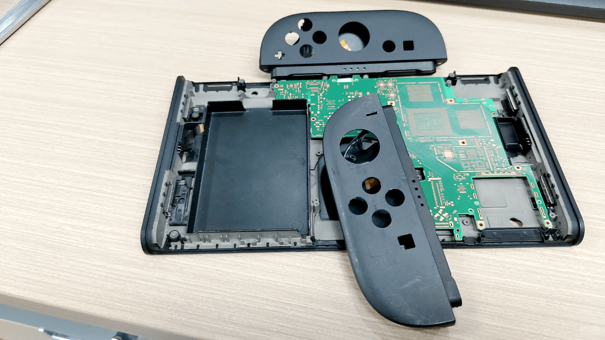
The eight-inch LCD. The larger form factor. The new Joycons connecting via magnetic rails. At this point we can assume it’s all true. Following up on the leak came a very interesting video from Xiao Ning Zi, who appears to have had access to the same CAD modelling info as last week’s leaker and has gone on to print out a model, which the channel has then compared to the OLED model, showing how substantially larger it is. The channel also makes performance claims, but much of this is not backed up by any visible sourcing – and I note several clips from the video that come from my own T239 video from earlier in the year.
- 0:00:00 Introduction
- 0:01:08 News 1: Switch 2 hardware revealed in apparent leak
- 0:23:07 News 2: Dragon’s Dogma 2 patch boosts PC performance
- 0:33:04 News 3: Dead Rising Deluxe Remaster tested
- 0:44:34 News 4: RDNA 4 skips high-end GPUs, FSR 4 to be AI-based
- 1:00:40 News 5: Intel, AMD battled over PS6 contract
- 1:07:32 News 6: Horizon, Days Gone remasters rumoured
- 1:17:50 News 7: John gets a Virtual Boy!
- 1:27:12 Supporter Q1: How does Sony deliver consistently good PC ports?
- 1:32:51 Supporter Q2: What do you make of Nintendo suing for Palworld’s alleged patent violations?
- 1:38:25 Supporter Q3: Would you expect to see a big difference between FSR 2 and PSSR on Pro titles? Is ML-based upscaling powerful enough to keep console prices low?
- 1:43:59 Supporter Q4: What benefits will PS5 Pro bring to the PlayStation Portal?
- 1:46:24 Supporter Q5: Will PS5 Pro titles bring back-compat boosts for PS6?
- 1:49:28 Supporter Q6: How likely is a 40fps PS5 Pro mode for GTA 6?
- 1:53:57 Supporter Q7: Why has Respawn failed to fix fundamental issues in Jedi: Survivor on PC?
- 1:59:44 Supporter Q8: Why isn’t there an Ernest-based game?
Here’s what else we can confirm at this point, based on the prototype leak, at least. Switch 2 has twin USB-C ports top and bottom (Xiao Ning Zi suggests the top one may be for peripherals including an external camera, while our own John Linneman suggests a use-case for charging while in table-top play). It’ll also have a Micro-SD card slot – and we’d hope it supports the latest and greatest formats to allow for bandwidth-heavy games to run. Otherwise you’re reliant on the 256GB of UFS 3.1 storage contained therein. Cartridges are supported too, with strong hints that original Switch media is also supported.
The fact that we’re getting an internal view of the Switch 2 is also highly revealing. The mainboard – shown without any of the chips mounted – gives us some idea of the architecture within. There are two pads for the 6GB LPDDRX 7500MT/s memory modules to sit on, giving us 12GB of RAM in total. A 128-bit memory interface offers up a maximum of 102GB/s of bandwidth, assuming Nintendo runs the RAM at full speed. Next to that is the area on which the highly contentious SoC sits – and therein the controversy heats up. Does the size of the area occupied by the SoC package give us any hints as to the technology used to make the chip?
The existence of Nintendo’s T239 processor was first revealed by renowned leaker kopite7kimi, way back in 2021. He called it a customised version of the T234 chip created by Nvidia for its automotive endeavours and also for its latest Jetson Orin NX kits. However, the links between T234 and T239 need to be brought into question. Since the publication of my T239 piece, sources have come forward to suggest that one is not derived from the other and that they were not developed by the same team. T239 is entirely custom for Nintendo, but is using RTX 30-series Ampere-architecture GPU cores with some RTX 40-series power saving and media features. The CPU is entirely different and it has a custom file decompression block for super-fast loading and data processing.
The controversy comes from the process node technology used to make T239 – crucial information which has still not leaked. Speaking to DF Supporter Program members on our Discord, I shared an image I generated in Photoshop which extrapolates the mainboard view into a top-down perspective. Despite the disclaimers I added, this image ended up on Reddit and from there, further theory-crafting emerged. The memory modules are 14mm by 14mm, so if we know how large T239 is (by comparing the SoC area to the memory area), we should be able to get some idea of the size of the chip and maybe the process node it is using. And that could be somewhat crucial, as the leaked prototype image shows a relatively small battery bay. Acknowledged handheld expert Cary Golomb noticed the same thing – since battery life is king, something has to give, and that would be performance.
The concept of an 8nm T239 is reluctantly understood by some to be a likely candidate for Switch 2 – which would be unfortunate, as it’s an old node at this point that is hardly power efficient. The automotive T234 is actually 455mm2 (!) which many believe rules it out completely as even a cut-back version would be too large, while Jetson power estimators suggest consumption that would never work on a handheld device. That said, a 2560 CUDA core RTX 3050 on the same node is around 200mm2, so a Switch 2 chip with 1536 CUDA cores would occupy around 60 percent of the space – enough area remaining for the ARM CPU cores and other ‘uncore’ components. The package size on the mainboard could accommodate that, but then again, it could accommodate any of the viable nodes.
Does the Jetson power estimator completely rule out an 8nm handheld? The evidence looks compelling, but the T234 chip is built by a different team for an entirely different application and it’s also a vast 455mm2 processor. T239 will be a far smaller processor that would have been built for Nintendo with handheld play in mind, designed specifically for the process node it uses – whatever that is. If 8nm was the target, the designers would have to work with that. Comparisons between T239 and T234 may be less relevant than expected, so power calculations from the estimator may not apply, especially as power-saving features from later Nvidia technology have been added.
An alternative train of thought is that – and this would be a first – Nintendo is using the same TSMC ‘4nm’ node used for the RTX 40-series graphics cards. This is actually a 5nm process, renamed by Nvidia and TSMC, presumably for marketing reasons. This would deliver incredible efficiency, fast clocks and tiny die area. But it is still a relatively recent process and we have to go all the way back to 2005’s Xbox 360 to see a console maker use the latest chip fabrication technology.
Typically console makers ‘wait their turn’ for this kind of technology (5nm is still in demand) and historically, Nintendo has used this to its advantage with the second generation ‘Mariko’ Switch that vastly improved battery life and made the smaller, Switch Lite possible. It may make sense for Nintendo to wait for a 4nm refresh – it would be much cheaper and more impactful further on in the Switch 2’s life cycle.
But the more you think about 4nm in the here and now, the more questions arise. If T239 was designed for 4nm, why not use the RTX 40-series Ada Lovelace GPU architecture to begin with? I’d also start wondering why Switch 2 is so much larger than its predecessor, bearing in mind that 4nm is incredibly efficient. The obvious explanation is that the new console is larger because it needs to dissipate more heat and I would expect a smaller unit based on this technology. So what are the alternatives? Chances are that the mainboard we’ve seen could house an 8nm processor, but just how slow would it run? Occam’s Razor, therefore, would suggest that the 6nm used by PS5 would be a better fit and it is available at a reasonable price for Nintendo – but Nintendo doesn’t have a history of sticking to ‘the rules’ or using the most plausible technology.
Another theory is that Switch 2 is so large to accommodate a 1080p screen, as opposed to housing a larger main processor. However, what the visualisations we’ve seen fail to communicate well is that there’s actually a sizeable bezel around the display, similar to the original Switch. If housing the eight-inch display is the reason for the larger handheld, I’m not sure it needs to be that big… unless the screen is actually larger. Heat dissipation still seems like the more plausible explanation then, suggesting a more realistic choice of process node.
Beyond that, historically, for Nintendo, price is everything. Similar to the original Switch – which also shipped on a less than ideal process – Switch 2 may well sit on 8nm. Original leaker kopite7kimi believes so – and maybe Nvidia and Nintendo may have arranged a ‘sweetheart’ deal with Samsung for this process, as opposed to the more logical 6nm alternative.
Truth is, we don’t know, but the thing about anticipation is that we always want the product to be the best it can possibly be and the unfortunate truth is that there is precedent for over-estimating the capabilities of new Nintendo hardware with each and every generation from the Wii onwards, even though Nintendo has proven time and time again that it doesn’t need the best possible tech. Even with Switch, few believed that Nintendo would use a vanilla Tegra X1, residing on the failed 20nm process. Tegra X2 on 16nm with double the bandwidth would have been a far better fit, yet TX1 it was.
Ultimately, we need to accept that Nintendo and Nvidia know what they are doing. Despite the limitations of Tegra X1 and a mostly awful showing on the Shield Android TV mini-console, Switch went on to become a phenomenal success and while games can clearly suffer from the limitations of the hardware (particularly the bandwidth situation that TX2 would have vastly improved), we’ve dined out on seven years worth of excellent releases, including an array of titles we’d never have believed possible on 2015-era mobile technology.
And now Nintendo faces the biggest challenge of all – somehow following that up.